
Speakers
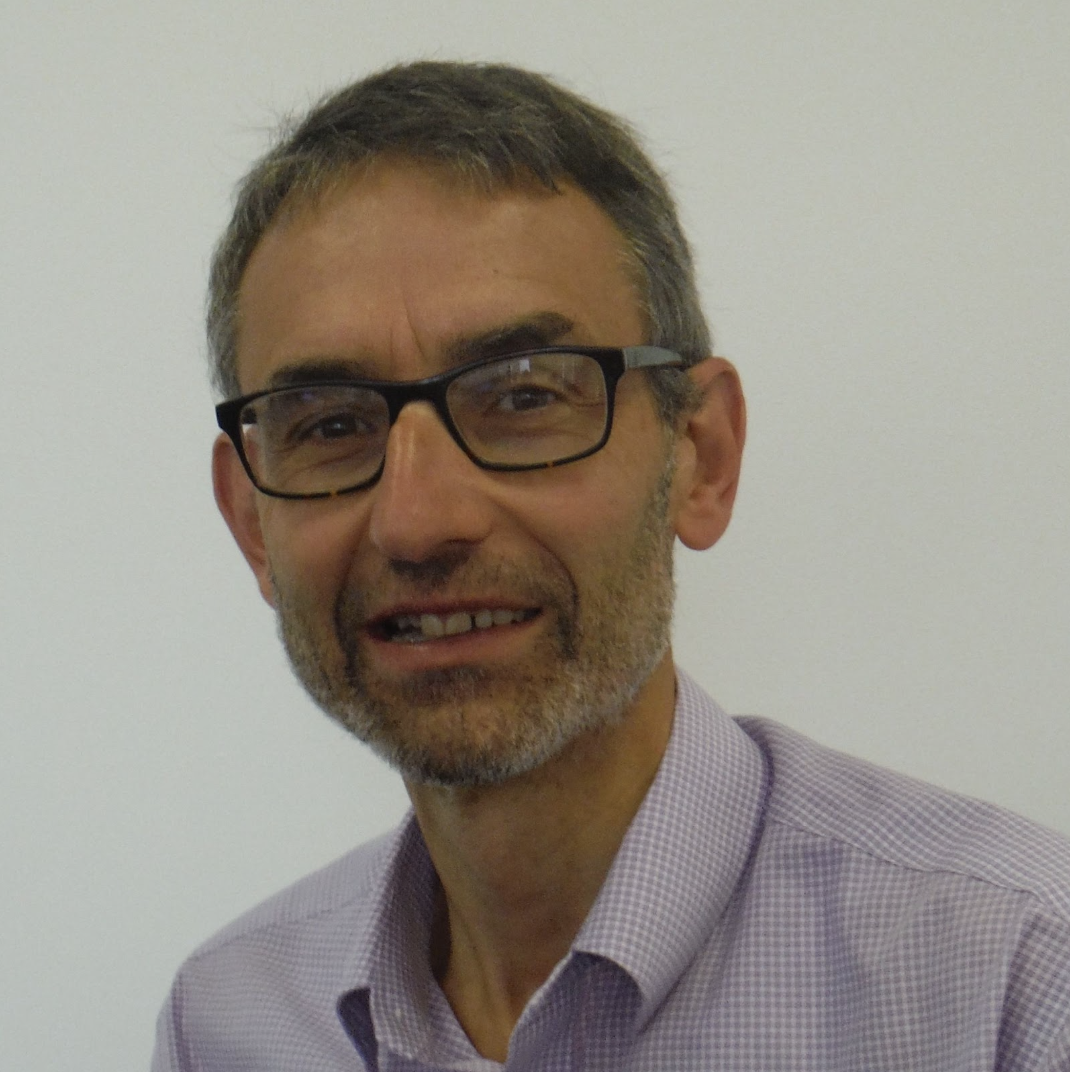
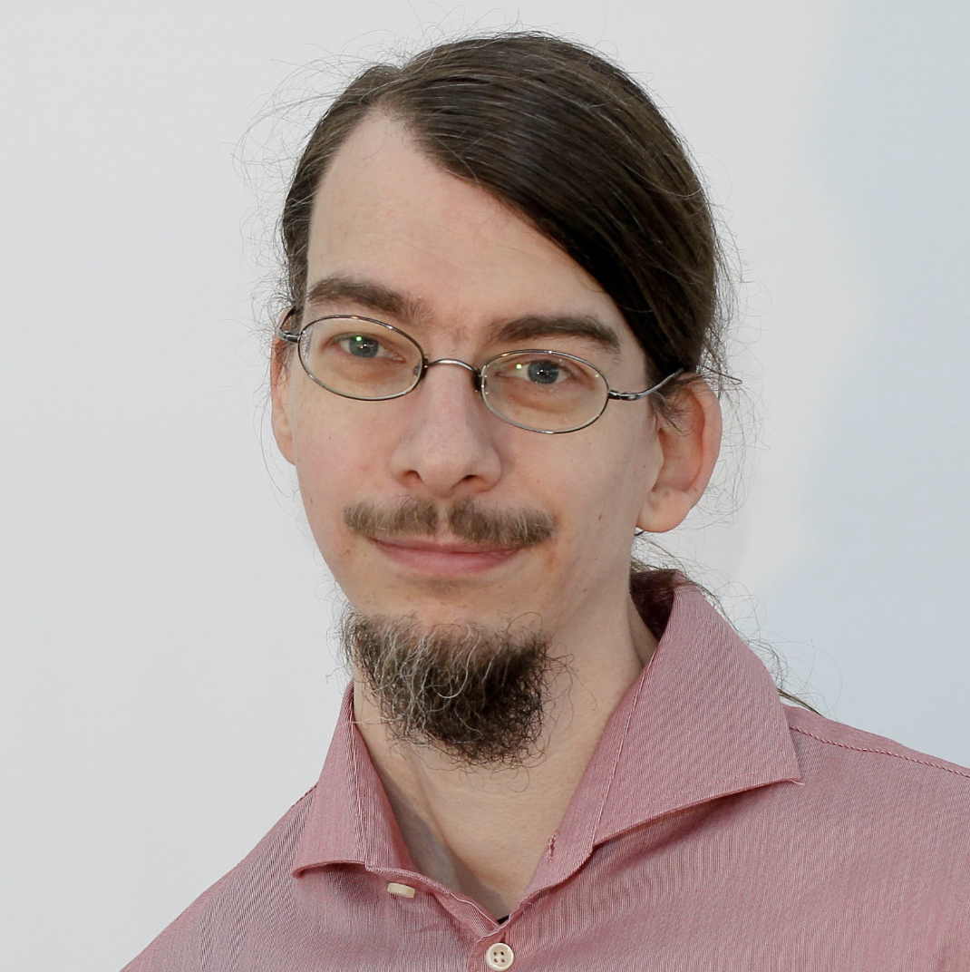
Dr. Jens Bolten (M) obtained both his diploma and his PhD in electrical engineering from Rheinisch-Westfälische Technische Hochschule (RWTH) Aachen, Germany. In 2006 he jonied AMO as a research engineer and is currently head of AMO´s nanostructuring team. His research focusses on high resolution electron beam lithography for electronic devices and the investigation of process integration, both with respect to a heterogeneous processing environment and to the integration of novel materials into pre-existing process modules and flows. He will oversee the process development and integration at AMO on a day-to-day basis.

Dr. Ivan Marozau (M) received his PhD in materials science from ETH Zurich (Switzerland) in 2009. Since 2015 he joined the “Materials science and Component Reliability” sector at CSEM as R&D engineer. He is responsible for the reliability testing and failure mode analysis activities at CSEM. He has an experience in reliability testing of MEMS and MOEMS components, their characterisation and failure mode analysis. In this project he will perform functional testing and reliability assessment of NEMS-based components
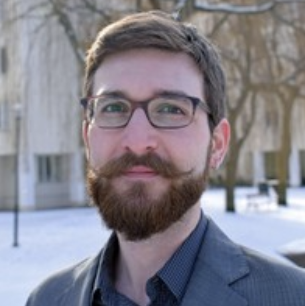
Simon J. Bleiker received his M.Sc. degree in electrical engineering from the Swiss Federal Institute of Technology (ETH) in Zurich, Switzerland in 2012 and his Ph.D. degree from the Royal Institute of Technology (KTH) in Stockholm, Sweden in 2017. His expertise lies in 3D-integration and packaging of MEMS and NEMS technology. Simon has published major contributions in the fields of nano-electromechanical switches, low temperature wafer bonding, self assembly, and through-silicon vias (TSVs). Currently, he is continuing his research on NEM switches and 3D integration in the department of Micro and Nanosystems at KTH Stockholm.
Dr. Yingying Li received her MSc in Precision Instrument from Tsinghua University, China, in 2021, and has since been pursuing a PhD in Micro and Nanosystems at the Royal Institute of Technology (KTH), Sweden. Her work bridges device-level fabrication and circuit-level integration, with expertise in the nanofabrication and wafer-level integration of nanoelectromechanical switches across commercial CMOS foundry platforms.
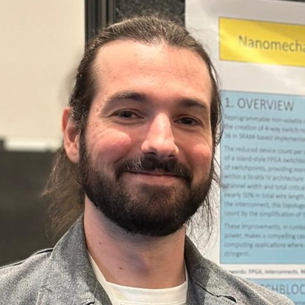
Dr. Victor Marot received his MSc in Advanced Microelectronic Systems Engineering in 2019 and his PhD in Electrical and Electronic Engineering in 2025, both from the University of Bristol. His PhD research has focused on the design, optimisation and characterisation of NEM digital circuits, contributing to the research of the i-Edge project. He currently furthers this research topic within the project, with a stronger focus on characterisation




i-EDGE has received funding from the European Union (grant number 101092018), the Swiss State Secretariat for Education, Research and Innovation (SERI) and UK Research and Innovation (UKRI) under the UK government's Horizon Europe funding guarantee (grant numbers 10061130 and 10063023).
Views and opinions expressed are however those of the author(s) only and do not necessarily reflect those of the European Union, European Health and Digital Executive Agency (HADEA), SERI or UKRI. Neither the European Union nor the granting authorities can be held responsible for them.