The technology behind i-EDGE
The i-EDGE project will develop electronic circuitry designed to withstand harsh environmental conditions in which conventional CMOS electronics can not be operated, namely high temperatures of up to 300 °C and high radiation levels of up to 1 Mrad. At the same time our circuits will have a negligible standby power consumption. As such, this technology is ideally suited to be co-integrated with sensors in System-on-Chip (SoC) devices for industrial IoT. Its unique properties enable us to address a range of demonstrators from different technological fields and industries, described in more detail here.
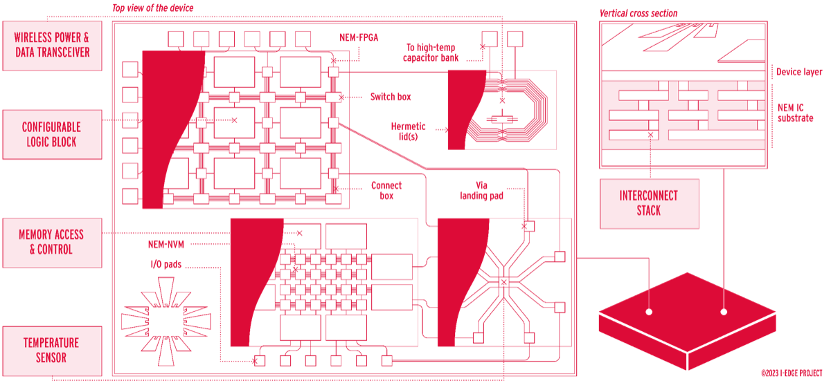
This will be achieved by exploiting device concepts based on nanoelectromechanical switches (NEMS) initially developed in a predecessor project, ZeroAMP. NEM switches, also called NEM relays, can, from a functional point of view, be seen as the nanomechanical equivalent of a transistor. Depending on a voltage applied to a gate contact a current flow between a source and a drain contact can either be switched on or off. By combining different basic NEM switch designs, this technology can be exploited to realize logic functions as well as volatile and non-volatile memory cells. Hence, the technology enables the integration of elements such as field programmable gate arrays (FPGAs), memory, memory access circuits and other elements such as basic sensors or readout circuitry on a single silicon chip.
While certain NEMS specific process steps are developed, the fabrication process flow for i-EDGE devices will still be very similar to conventional CMOS device manufacturing. This allows the project not only to heavily rely on well-established fabrication techniques such as lithography or dry etching, but also enables the use of commercially available silicon foundry services as part of its integration approach. This not only reduces costs for the fabrication of initial prototypes of the project’s first demonstrators, but also provides a clear path from lab-scale device fabrication by the project consortium to a commercially relevant manufacturing of SoC targeted competitive products. Initially, device fabrication will be shared between UNIVBRIS, KTH and AMO and utilize the infrastructure available to the consortium. At the same time, our process flows are all developed having an easy and smooth transition into a fabless silicon-foundry based manufacturing approach in mind.
At the same time, the project will also further develop a process design kit (PDK) originally initiated as part of the ZeroAMP project. Like CMOS or photonic PDKs, it will allow future users of our technology easy access to its functionality by using predefined elements. This enables circuit designers to concentrate on the functionality of the desired circuits, without the need to deal with the actual layout of single NEM switches or basic elements such as a memory cell. Hence, the technology developed in i-EDGE will have a low access hurdle and allow for an easy early adoption by interested third parties.
i-EDGE has received funding from the European Union (grant number 101092018), the Swiss State Secretariat for Education, Research and Innovation (SERI) and UK Research and Innovation (UKRI) under the UK government's Horizon Europe funding guarantee (grant numbers 10061130 and 10063023).
Views and opinions expressed are however those of the author(s) only and do not necessarily reflect those of the European Union, European Health and Digital Executive Agency (HADEA), SERI or UKRI. Neither the European Union nor the granting authorities can be held responsible for them.


